The website is underconstruction, so the project is yet to be updated.
Below is a timeline outlining all of the major publications related to the development of single-pixel THz cameras that were performed by this research group. The theory about single-pixel imaging can be found at [link is missing…].
We report the first use of a convolutional neural network for terahertz (THz) imaging combined with a single-pixel camera to achieve high quality hyperspectral THz imaging 10x faster than the current commercial systems, with faster potential only limited by noise. Imaging with a spatial light modulator (SLM) relies on projecting a set of spatial patterns onto an object and recording the transmission with a single-pixel detector, and an optical delay unit (ODU) is used to obtain the terahertz time-of-flight information. A key breakthrough in this work is to synchronize the equipment to not need any time to instruct the ODU to move while projecting the patterns. See full publication at ACS Photonics 2021, 8, 11, 3150–3155.
November
Terahertz (THz) radiation is poised to have an essential role in many imaging applications, from industrial inspections to medical diagnosis. However, commercialization is prevented by impractical and expensive THz instrumentation. Single-pixel cameras have emerged as alternatives to multi-pixel cameras due to reduced costs and superior durability. Here, by optimizing the modulation geometry and post-processing algorithms, we demonstrate the acquisition of a THz-video (32×32 pixels at 6 frames-per-second), shown in real-time, using a single-pixel fiber-coupled photoconductive THz detector. A laser diode with a digital micromirror device shining visible light onto silicon acts as the spatial THz modulator. We mathematically account for the temporal response of the system, reduce noise with a lock-in free carrier-wave modulation and realize quick, noise-robust image undersampling. Since our modifications do not impose intricate manufacturing, require long post-processing, nor sacrifice the time-resolving capabilities of THz-spectrometers, their greatest asset, this work has the potential to serve as a foundation for all future single-pixel THz imaging systems. See full publication at Nature Communications, vol 11, Article number: 2535 (2020).
May

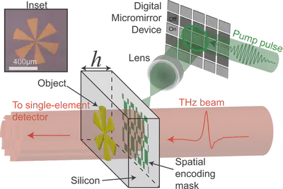
We demonstrate a form of near-field terahertz (THz) imaging that is compatible with compressed sensing algorithms. By spatially photomodulating THz pulses using a set of shaped binary optical patterns and employing a 6-μm-thick silicon wafer, we are able to reconstruct THz images of an object placed on the exit interface of the wafer. A single-element detector is used to measure the electric field amplitude of transmitted THz radiation for each projected pattern, with the ultra-thin wafer allowing us to access the THz evanescent near fields to achieve a spatial resolution of ∼9μm (λ/45 at 0.75 THz). We conclude by experimentally improving the image rate by a factor of ∼3 by undersampling the object with adaptive and compressed sensing algorithms.. Full publication at Optica Vol. 4, Issue 8, pp. 989-992 (2017).
August
Terahertz (THz) imaging can see through otherwise opaque materials. However, because of the long wavelengths of THz radiation (λ = 400 mm at 0.75 THz), far-field THz imaging techniques suffer from low resolution compared to visible wavelengths. We demonstrate noninvasive, near-field THz imaging with subwavelength resolution. We project a time-varying, intense (>100 mJ/cm$^2$ ) optical pattern onto a silicon wafer, which spatially modulates the transmission of synchronous pulse of THz radiation. An unknown object is placed on the hidden side of the silicon, and the far-field THz transmission corresponding to each mask is recorded by a single-element detector. Knowledge of the patterns and of the corresponding detector signal are combined to give an image of the object. Using this technique, we image a printed circuit board on the underside of a 115-mm-thick silicon wafer with ~100-mm (λ/4) resolution. With subwavelength resolution and the inherent sensitivity to local conductivity, it is possible to detect fissures in the circuitry wiring of a few micrometers in size. THz imaging systems of this type will have other uses too, where noninvasive measurement or imaging of concealed structures is necessary, such as in semiconductor manufacturing or in ex vivo bioimaging. Full publication at Science Advances, Vol 2, Issue 6:e1600190.
June